Caution while doing inverter repairing
- Don’t touch 12v and Sw (switch) pin otherwise microcontroller may become dead or faulty. To switch on the inverter short the Sw and ground pins only. Video
- Always check the gate resistance (36 to 50 ohm) after installing the new mosfet.
- If you are changing the IC or inspecting the Mosfet be sure that the mosfet is receiving the correct voltage from the IC, otherwise IC might be faulty. Video reference
- Never put 12v mosfet in 24v pcb system, but you can do the reverse.
Components of Inverter and testing
-
Battery selector switch
-
Display PCB
-
Fan
-
Five Pin socket + Resistor (250Ω)+Capactors in series
-
Fuse
-
Main switch (For On off)
Shorting the +12v and SW turns on the pcb circuit of inverter.- Different inverter pcb use different system to switch on the PCB.
-
PCB
-
Battery connecting socket – B+/B-
-
BJT Transistor – Q1
- Instead of BJT transistor/drive transistor a mechanic is using diode to solve the problem. Video.
-
Buzzer – Buz1
-
Capacitor – C1
-
Connectors – CN1
- e.g On a PCB (Printed Circuit Board), the label CN2 refers to the second connector on the board.
-
Crystal oscillator – X1
-
Diode – D1
- Instead of BJT transistor/drive transistor a mechanic is using diode to solve the problem. Video.
-
Fuse – F1
-
Fuse Diode – FD1/FD2
- In a battery inverter PCB, FD2 typically refers to a point associated with a fuse diode or a fuse holder, which is used for overcurrent protection. The “FD” designation generally indicates a fuse-related component, and the number following it (in this case, 2) differentiates it from other fuse components on the board.The purpose of this component is to protect the circuit from damage caused by excessive current. If the current exceeds a certain threshold, the fuse will blow, interrupting the circuit and preventing further damage to the inverter or its components.
-
Heat Sink – HS1
-
IC – U1
- There can be many ic or microcontrollers in the inverter pcb e.g.
- 28 Pin microcontroller
- This microcontroller controls the entire function of the inverter
- A continous beep shound will generate if there is 5v missing in point 1 and point 20 of this microcontroller.
- A transistor named 7805 mosfet converts 12 v to 5 v and then it powers the 28 leg microcontroller in sukam inverters. But Luminous inverter use Three leg IC to power the 28 Leg microcontroller.
- Luminous inverter 28 leg full details. Video.
- Microtek EB 900 sine wave inverter 28 leg pin details – Video
- 83202 IC

- About 83202 IC.
- 83202 PDF.
- If 83202 ic becomes short then also overload error occurs
- If the pin 6 and 12 shorted then there should be no continuity or short. If this is the case then 83202 ic is correct.
- Working of 83202 video.
-
In system programming – ISP1
- “ISP1” usually stands for In-System Programming. This indicates a programming port for microcontrollers or other programmable components on the PCB. ISP allows for the firmware or software to be updated directly while the component is installed in the circuit, which is particularly useful for debugging or upgrading the inverter’s functionality
-
IGBT Transistor – Q1
-
Jack – J1
- In the context of a PCB (Printed Circuit Board), the designator J1 typically refers to a jack or connector. These designators are part of a standardized system used in electronics to identify various components on the board.
- J1 indicates the first jack connector on the PCB, where external devices or cables can connect to the circuit. This might include connectors for power supply, signal input, or output.
- In the context of a PCB (Printed Circuit Board), the designator J1 typically refers to a jack or connector. These designators are part of a standardized system used in electronics to identify various components on the board.
-
Jumper position – JP1
- In PCB design, “JP1” typically stands for “Jumper Position 1.” Jumpers are used to establish connections between two or more points on a circuit board, allowing for configuration options or enabling/disabling certain functionalities. Each jumper is labeled with a reference designator like JP1, JP2, etc., to indicate its specific location and purpose.For instance, if a PCB has multiple jumpers, they might be used for selecting different modes of operation, configuring voltages, or setting up hard ware options. The label “JP1” would help engineers and technicians quickly identify and understand the function of that jumper during assembly, troubleshooting, or modification(
-
Mosfet Transistor – MS1 or Q1
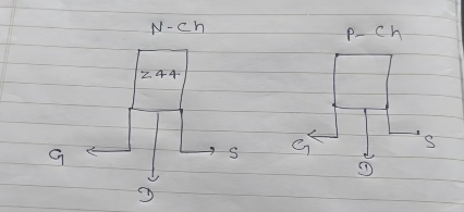
- In N channel mosfet the input (voltage or signal) is given from Drain to source and vice versa in P channel.
- Inverters use only N Channel Mosfets such as p55, z44, psc
- A good mosfet shows no shorting or continuity in any three points of GDR.
- Here is the process to check mosfet from multimeter. Video.
- In an inverter, when checking the MOSFET before the voltage or signal enters the gate point, there is always a resistance ranging between 36 to 50 ohms. If you are checking the mosfet you should also check the resistance also.
- There should be a voltage of 4 to 4.5 v between battery – and mosfet ground point where the drain wires of the transfomers are connected or not connected.
- There should be a voltage of 12V between battery – and mosfet ground point in which the red wires is connected to the heatsink, when the inverter is in backup mode and the voltage should be 4 to 4.5 volt when the inverter is in charging position. Video.
The IC such as 80202 IC or 83202 IC powers the Mosfet which converts battery 12 v to 4 to 4.5 and provide voltage to Mosfet.If you are changing the IC or inspecting the Mosfet be sure that the mosfet is receiving the correct voltage from the IC, otherwise IC might be faulty. Video reference- Mosfets comes in different current range such as 40A, 60A and 80 A
- Mosfet checking: If the mosfet is correct there should be 10.5 volts ac between both the terminals of the drain wires. If less voltage or no voltage try checking the mosfet in other way or other components of mosfet connected.
- Mosfet blast due to high voltage and due to heavy voltage variation.
-
Mounting Hole – MH1
- MH1 designation typically stands for a mounting hole. Mounting holes are used to physically secure the PCB in a chassis or enclosure, helping to stabilize and support the board during operation.
-
MOV (Resisitor) – MOV
-
Negative Temperature Coefficient (NTC) thermistor – NTC1
- An NTC (Negative Temperature Coefficient) thermistor in a battery inverter is a temperature-sensitive resistor that is commonly used to protect the system from overheating and to monitor temperature and commands inverter fan to switch on when heat sink temperture rises.
-
Neutral – Negative wire socket
-
Octocoupler IC – U1
-
Relay – RL1 or K1
- There are two relay in inverter because….
- Seamless Transfer Between Power Sources: One relay manages the transfer between mains power and inverter power. When the grid power is available, it connects the load directly to the mains, bypassing the inverter to conserve battery. When the mains fails, the relay switches to battery mode, allowing the inverter to power the load.
- Overload and Safety Protection: The second relay handles the switching of the inverter’s AC output to the appliances and provides necessary protection for the inverter system. It disconnects the load in case of overload, low battery voltage, or faults, safeguarding the system.
- In normal working condition if one relay is on then second relay should have no voltage in terminals and should be switched off.
- Relays can be controlled by main IC (28 leg e.g. sukam inverter) or separate IC (ULN2003AN e.g luminous)
- In Luminous inverters both the relay is controlled by IC such as ULN2003AN and faulty relay IC may result in malfunction of the relay
-
Resistor – R1
-
Serial Number – S/N:
-
Shunt resistance – SH1
- In the context of an inverter PCB, SH1 typically refers to a “shunt” or “shunt resistor.” Shunt resistors are used to measure current by creating a small voltage drop that can be measured without significantly impacting the overall circuit. This allows for accurate current sensing, which is essential for monitoring performance and protecting the inverter from overload conditions.The designator “SH” is commonly used for shunts in circuit schematics and PCBs, followed by a number to distinguish between multiple shunts present on the board (e.g., SH1, SH2). This labeling system helps ensure clarity and organization in the PCB design, making it easier to identify and troubleshoot components.
-
SMD Bridge rectifier – MB/DB/AB/AF
-
T Sns
- This is also a temperature sensor resistor in the inverter pcb which commands fan operation.
-
-
Transformer – T1
-
UPS/WUPS Switch
Component testing of Inverter shifted to Components of Inverter and testing
OK

OK

Gate drive Checking process
- Always check the Gate resistance and gate diodes properly after installing new mosfet
- Voltage between the Battery black wire and the gate (pin 1) of the drain side mosfet should be around 3 volts. Or it should be 4 to 4.5 in some other inverters in (pin 1) of the drain side mosfet when inverter is in non Charging or in Backup mode.
- You should definately change the 80202 or 832020 IC or some other Pulse generating IC (Depends on Inverter model) after changing the mosfets. (Because the 80202 or 832020 IC gets shorted upon Mosfet blast.)
- There should be a voltage of 12V between battery – and mosfet ground point in which the red wires is connected to the heatsink, when the inverter is in backup mode and the voltage should be 4 to 4.5 volt when the inverter is in charging position. Video.
- If you are changing the IC or inspecting the Mosfet be sure that the mosfet is receiving the correct voltage from the IC, otherwise IC might be faulty.
- If gate drive volt is not correct then install new mosfet only after correcting the gate drive voltage only.
- If the gate drive of the mosfet is not correct then you should check all the resistors diodes capacitors from the Main IC to Mosfet. Reference.
- While checking the mosfets if two mosfets have slightly different drive voltages that means
Reasons Why Gate Drive Voltages May Differ:
-
Different MOSFETs used:
-
Gate Resistors Mismatched:
-
Unequal gate resistors can cause voltage drops or differences in charging the gate capacitance.
-
-
Gate Drive Circuit Problem:
-
If the gate driver IC or driver transformer is not distributing equal voltages, you’ll see variation.
-
-
PCB Layout Issues:
-
Long or different trace lengths to gate pins may cause unequal voltages due to inductance or resistance.
-
-
Gate Leakage or Short:
-
If one MOSFET is partially shorted (Gate to Source), it can pull down the voltage.
-
-
- Correct drain voltage can be also checked like this with volt btw 11-11.80 volt.
- If you are not getting drive in the mosfet this is how you can confirm that Microcontroller IC is ok or not . Link.
Home Inverter connection
- Inverter connection for home
Inverter Wires color code
| DC + | Red |
| DC – | Black |
| AC + (Live) | Red |
| AC – (Neutral) | Black |
| AC Earthing | Green |
Inverter parts purchase online websites
Inverter sections
Here is the short explaining the sections of the inverter such as
- Batteru section
- Charging section
- Inverter section
- Controller section – voltage current load over load etc
- Change over section e.g relay
- Protection section
Making of inverter

PCB Reference designators list
- More details…about pcb designators symbols
- Another website tell all the symbols designated to pcb components
| TABLE OF STANDARD PCB REFERENCE DESIGNATORS | ||||
| Reference Designator | PCB Element | Reference Designator | PCB Element | |
| A | Assembly | PS | Power supply | |
| AN, AS | Antenna | Q, TR | Transistor | |
| AR | Amplifier | R | Resistor, potentiometer | |
| B | Battery | RT | Thermistor | |
| BR | Bridge rectifier | RLA, RY | Relay | |
| BZ | Buzzer | S, SW | Switch | |
| C | Capacitor | TP | Test point | |
| CB | Circuit breaker | TR | Transistor, transducer | |
| D | Diode | U | IC, inseparable assembly | |
| M | Meter, measuring device | W | Cable, wire, busbar | |
| MH | Mounting hole | XTAL | Crystal rectifier | |
| OP | Operational amplifier | XMER | Transformer | |
| P | Plug | Y | Crystal oscillator | |
Playlist of Inverter repair
Questions and Doubts
- What is the use of 555 Timer IC in inverter ?
A Timer IC, such as the 555 timer, is used in inverters for generating precise timing pulses to control the switching of transistors or MOSFETs. This enables the inverter to convert DC to AC at a stable frequency, essential for consistent power output. - What causing inverter to overload without any real load when switched on ?
- How to find if the mosfet is N channel or P channel ?
- What is the use of driver IC in inverter ?
- Difference between two and three channel inverters ?
- How to find if the transistor is PNP or NPN ?
- Why 2 relays in inverter PCB ?
- How to check pcb transformer ?
- Inverter is not charging the battery and turns off after the mains is gone or very less time backup ?
- in Su Kam shark 850 inverter pcb there is written mov1, c35 and k2 near a single component. what does that mean ?
- What is 1 to 1 inverter card ?
- What is v4 v5 v6 v7 smd board
Ans – V4, V5, V6, and V7 SMD boards are commonly used as microcontroller or inverter control modules in various electronic products, including sine wave inverters. Each version typically represents incremental improvements in design, processing power, or compatibility. For example, the Microtek V4, V5, V6, and V8 boards are used in inverter kits, where they function as core SMD microcontrollers, managing functions like signal processing and load control for optimized performance and efficiency in power management systems - How is drive pulse is generated in inverter ?
Ans – Watch this video to understand how the drive pulse gets generate in Microtek inverter pcb. - What is triac and 555 timer and scr in inverter ?
In an inverter, components like a TRIAC, 555 timer, and SCR (Silicon Controlled Rectifier) play essential roles in switching, timing, and controlling power to convert DC into AC effectively. Here’s a breakdown of what each of these components is and their roles in inverter circuits:1. TRIAC (Triode for Alternating Current)
- A TRIAC is a semiconductor device that can conduct current in both directions (forward and reverse), which makes it suitable for AC power control.
- In an inverter circuit, the TRIAC acts as a switch that controls the AC output by turning on and off at specific intervals to create an alternating current waveform.
- TRIACs are widely used in low to medium-power AC control applications because they allow control of AC loads with simple triggering.
Role in Inverter:
- The TRIAC receives triggering signals to switch on and off periodically, allowing the creation of an AC waveform from a DC source. When used with a 555 timer, it can be controlled at a frequency of 50Hz or 60Hz, which is the typical frequency for AC power.
2. 555 Timer
- The 555 timer IC is a highly versatile integrated circuit used for generating precise time delays or oscillations (square waves).
- In inverters, the 555 timer often operates in astable mode to produce a continuous square wave output, which serves as the timing control signal for switching devices like TRIACs or MOSFETs.
- The frequency of the square wave output is usually set to match the desired AC output frequency (e.g., 50Hz or 60Hz).
Role in Inverter:
- The 555 timer sets the switching frequency of the inverter by providing a timing signal that determines when the AC output switches polarity. This is essential for simulating the AC waveform from a DC input.
3. SCR (Silicon Controlled Rectifier)
- An SCR is a unidirectional (one-way) semiconductor device that only allows current to flow in one direction once it’s triggered. After being triggered, it remains on until the current drops to zero.
- SCRs are typically used in high-power inverters and DC to AC conversion circuits where controlled rectification is needed.
- Unlike the TRIAC, which can switch in both directions, the SCR conducts only in one direction, making it ideal for phase control in DC-to-AC circuits.
Role in Inverter:
- SCRs are often used in the DC-to-AC conversion stage, particularly in high-power applications. They work in tandem with other control circuits (like a 555 timer) to create an AC waveform by alternately switching current directions. By carefully timing the triggering of SCRs, the inverter circuit can produce the desired alternating current output.
How They Work Together in an Inverter
- 555 Timer: Generates the low-power square wave signal at a set frequency.
- SCR or TRIAC: Acts as the switching device that controls power flow to the AC load, creating the AC waveform.
- Control Circuit: Combines these components to provide synchronized switching and control, turning DC into a simulated AC output.
In summary, the 555 timer provides timing signals, while the TRIAC or SCR handles the actual high-power switching to form the AC waveform from a DC source, each component working together to convert and control the power output.
Working of Inverter


Luminous inverter

Youtube inverter repair case study videos
- NA
Mains Voltage faults explained
Transformer Issue

Inverter repair tools
Charging section explanation
Display LED Problem
Low voltage output
Switch Problem
Reverse voltage output from AC input socket
Relay problem
Overload
Overheating
Overcharging
No charging
No voltage output from inverter back socket
Mosfet Blowing issue
Low battery Issue
Inverter going in mains mode when battery wires connected
Incorrect drive voltage in Mosfet
IC (28leg IC microcontroller) damaged or burnt
Humming sound
High Voltage output
Dead Inverter
Continous Fan Run
Continuous Beep sound
Battery connectors shorting
Battery charging Full issue
Inverter Issues